
welcome to buy Akeson® 8 Layers Thick Gold pcb Surface Finished Printed Circuit Boards Manufacturing PCBa one step sevice from us.
Akeson® 8 Layers Thick Gold pcb Surface Finished Printed Circuit Boards Manufacturing PCBa one step sevice
Specific
if have Gerber file or enquire. please email is violet(at)akesoncircuit(dot)com(dot) cn
Deliverables
1/Quotes in 24 hours or less
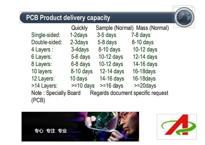
2/Standard production leadtime of 20 working days (4 weeks)
3/Prototype leadtime of 5 to 10 working days (1-2 weeks)
4/Stack-ups and impedance simulation in 36 hours
5/Initial response to technical questions or quality concerns in 36 hours
6/DFM and EQ's prior to PO placement upon request
Quality system
1/Akeson has mature and stringent Q
2/100% AOI, 100% ET, 100% FQC + FQA
3/SPC and Cpk programs
4/Lean Manufacturing and 6S programs
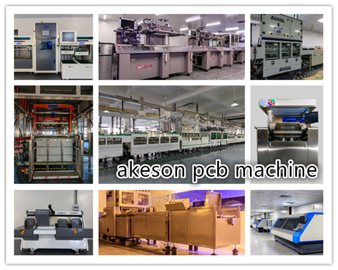
5/Advanced inspection and lab equipment
6/Standard QA report with every shipment
7/RoHS and REACH Compliance
8/Conflict Minerals Compliance
Products infomation
8 layer,
Material:FR4(Tg180) material,
PCB thickness:1.60mm thick,
Final copper:1 OZ finished copper on all layers,
Surface:ENIG surface finish,
Ttchnology:with hard gold finger at edge-board,
Solder mask:green solder mask,
with impedance control
6.0/7.0mil min w/s(line width/spacing),
min drill bit:0.20mm,
min BGA pad size:0.33mm
|
Product name |
Single side |
Double side |
4 layer |
6 layer |
8 layer |
10-28layer |
|
layer |
Single side |
Double side |
4 layer |
6 layer |
8 layer |
10-28layer |
|
Base Maerial |
CEM1,CEM3,FR1,FR3,ALU, FR4,polymide |
FR4,Alu,polymide |
FR4 |
FR4 |
FR4 |
FR4 |
|
Copper thickness |
1-6OZ |
|||||
|
Min.Hole size |
0.1mm |
|||||
|
Min.Line Width |
0.1mm |
|||||
|
Surface finishing: |
HASL / HASL lead free, HAL, Chemical tin, Chemical Gold, Immersion Silver/Gold, OSP, Gold plating |
|||||
|
Solder masker color |
green,red,black,white,yellow |
|||||
|
Silkscreen color |
black,white,yellow |
|||||
|
Tolerance |
- Shape tolerance: ±0.13 |
|||||
|
Special requirements |
Buried and blind vias+controlled impedance +BGA |
|||||


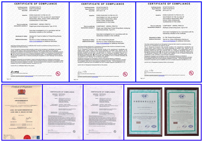
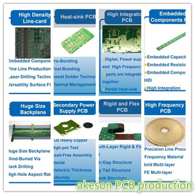
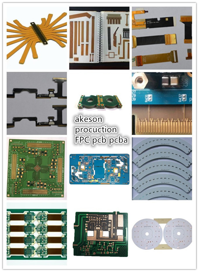

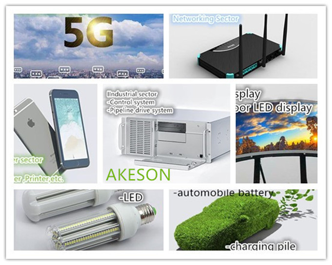

With superior technologies and facilities, strict quality command, reasonable cost, exceptional provider and close co-operation with customers, we've been devoted to delivering the best benefit for our buyers for Hot Selling for China Thick Gold Surface Finished Printed Circuit Boards Manufacturing PCBA One Step Sevice, We welcome shoppers, enterprise associations and mates from all sections of your environment to call us and seek out cooperation for mutual advantages. Hot Selling for China PCB Design, PCB Board, We accomplish this by exporting our wigs directly from our own factory for you. The goal of our company is to get customers who enjoy coming back to their business. We sincerely hope to cooperate with you in the near future. If there's any opportunity, welcome to visit our factory!