High-Density Interconnect (HDI) printed circuit boards represent a significant advancement in electronics manufacturing, enabling more powerful, compact, and reliable devices across numerous industries. This article provides a comprehensive overview of HDI PCB technology, its key applications, performance benefits, and technical specifications. We will explore detailed product parameters through structured lists and comparison tables, offering valuable insights for engineers, designers, and procurement specialists seeking to leverage HDI technology in their projects.
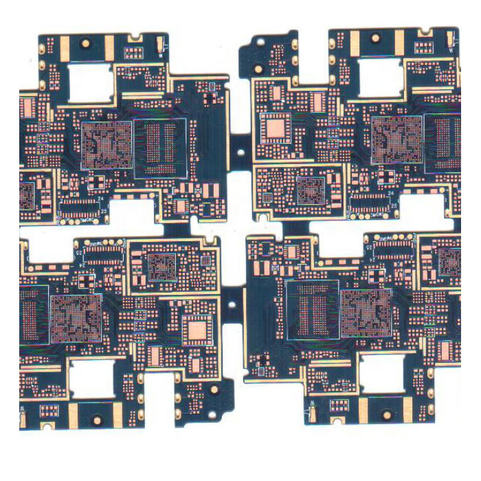
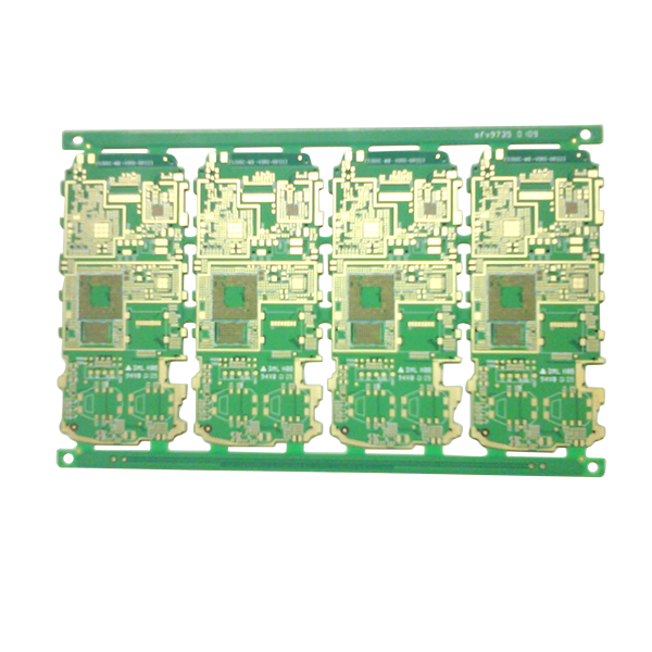
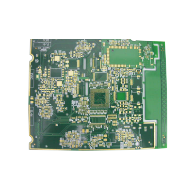
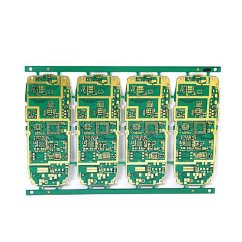
HDI PCB refers to a type of printed circuit board that offers higher wiring density per unit area compared to conventional PCBs. This is achieved through the use of finer lines and spaces, smaller vias, and higher connection pad density. These boards are characterized by microvias, blind and buried vias, and often involve multiple laminations to create intricate multilayer structures. The result is a compact, lightweight, and high-performance solution ideal for modern electronic devices where space and performance are critical.
HDI PCBs are used in a wide range of industries due to their ability to support complex designs and high-speed signals. Some of the most prominent applications include:
Consumer Electronics: Smartphones, tablets, laptops, and wearable devices benefit from the compact size and enhanced performance of HDI PCBs, allowing for slimmer designs and more features.
Medical Devices: Advanced medical equipment such as imaging systems, implantable devices, and portable monitors rely on HDI technology for reliability, precision, and miniaturization.
Automotive Electronics: Modern vehicles use HDI PCBs in infotainment systems, advanced driver-assistance systems (ADAS), engine control units, and sensors to improve functionality and safety.
Aerospace and Defense: HDI boards are essential in avionics, communication systems, and military equipment where high reliability, durability, and performance under extreme conditions are required.
Telecommunications: Networking equipment, routers, and 5G infrastructure utilize HDI PCBs to manage high-frequency signals and complex interconnect requirements.
Industrial Automation: Robotics, control systems, and IoT devices leverage HDI technology for improved signal integrity and space efficiency.
The adoption of HDI PCB technology offers several significant advantages:
Enhanced Signal Integrity:
HDI designs minimize signal loss and cross-talk through shorter pathways and better impedance control, which is crucial for high-frequency applications.
Improved Thermal Management:
The dense structure and advanced materials used in HDI PCBs help dissipate heat more effectively, increasing the lifespan and reliability of electronic devices.
Higher Reliability:
The use of microvias and stacked via structures reduces the number of through-holes and interconnections, lowering the risk of failure and improving overall durability.
Reduced Size and Weight:
HDI technology allows for more components to be placed in a smaller area, making it ideal for portable and miniaturized devices.
Cost Efficiency:
While initial manufacturing may be more complex, HDI PCBs can reduce layer count and overall system costs by integrating more functions into a smaller board.
To better understand the capabilities of HDI PCBs, below are the typical specifications and parameters offered by Akeson®:
Key Parameters List:
Layer Count: 4 to 20 layers
Board Thickness: 0.4mm to 3.2mm
Minimum Trace Width/Space: 0.05mm / 0.05mm
Via Types: Blind, buried, microvia (laser drilled)
Microvia Diameter: 0.075mm to 0.15mm
Copper Weight: 0.5oz to 3oz
Surface Finish: ENIG, HASL, Immersion Silver, OSP, ENEPIG
Dielectric Material: FR-4, High-Tg FR-4, Polyimide, Rogers, Isola
Minimum Pad Size: 0.25mm
Solder Mask: LPI (Liquid Photoimageable) in various colors
Comparison Table: Standard PCB vs. HDI PCB
| Parameter | Standard PCB | HDI PCB |
|---|---|---|
| Trace Width/Space | ≥ 0.1mm / 0.1mm | ≤ 0.05mm / 0.05mm |
| Via Size | ≥ 0.3mm | 0.075mm - 0.15mm (microvia) |
| Layer Count Efficiency | Lower | Higher (more functions per layer) |
| Signal Integrity | Moderate | Excellent |
| Typical Applications | Basic electronics | Advanced, compact devices |
| Cost Structure | Lower per unit area | Higher integration potential |
Advanced HDI Capabilities Table:
| Feature | Specification |
|---|---|
| Sequential Lamination | Up to 4 times |
| Via-in-Pad | Supported |
| Copper Filling | Available for thermal management |
| Impedance Control | ±10% tolerance |
| High-Frequency Materials | Rogers, Taconic, Arlon |
| Peelable Mask | Optional for selective soldering |
At Akeson®, we combine cutting-edge technology with decades of manufacturing expertise to deliver HDI PCBs that meet the highest standards of quality and performance. Our state-of-the-art facilities are equipped with laser drilling, automated optical inspection (AOI), and advanced testing systems to ensure every board meets precise specifications. We work closely with our clients to provide customized solutions that optimize performance, reduce time-to-market, and control costs.
HDI PCB technology continues to drive innovation across industries by enabling smaller, faster, and more reliable electronic products. Understanding its applications, advantages, and technical parameters is essential for making informed design and sourcing decisions. At Akeson®, we are committed to providing top-quality HDI PCBs that empower your innovations and help you stay ahead in a competitive market.
We invite you to experience the difference that professional HDI PCB manufacturing can make. For more information or to discuss your specific requirements, please reach out to our team at sale1@akesoncircuit.com.cn. Let’s build the future of technology together.