A Multilayer PCB is the backbone of modern electronic systems, enabling compact design, high-speed signal transmission, and superior electrical performance. As electronic devices become smaller yet more powerful, multilayer printed circuit boards have become an indispensable solution across industries such as telecommunications, automotive electronics, medical devices, and industrial automation.
In this in-depth guide, we will explore what a multilayer PCB is, how it works, its manufacturing process, advantages, applications, and key design considerations. We will also explain why partnering with an experienced manufacturer like Akeson is critical for achieving consistent quality and long-term reliability.

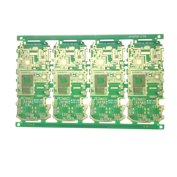
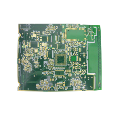
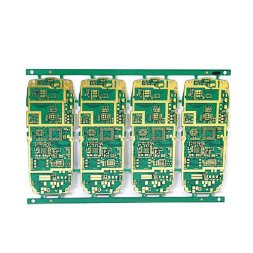
A multilayer PCB is a printed circuit board that consists of three or more conductive copper layers stacked together and electrically interconnected using plated through-holes or vias. These layers are separated by insulating materials such as prepreg and core laminates.
Unlike single-layer or double-layer boards, multilayer PCBs allow complex circuit routing within a compact footprint. This makes them ideal for high-density electronic designs where space, performance, and reliability are critical.
Learn more about multilayer PCB solutions on Akeson’s Multilayer PCB product page.
The structure of a multilayer PCB is carefully engineered to balance electrical performance, mechanical strength, and thermal stability.
| Layer Type | Function |
|---|---|
| Signal Layer | Routes electrical signals between components |
| Power Layer | Delivers stable voltage to components |
| Ground Layer | Reduces noise and improves signal integrity |
| Insulation Layer | Electrically isolates copper layers |
Multilayer PCB manufacturing is a precise and multi-step process that demands advanced equipment and strict quality control.
Any misalignment or material inconsistency during these steps can compromise the final PCB performance, which is why experienced manufacturers like Akeson invest heavily in process control.
| Feature | Single-Layer PCB | Double-Layer PCB | Multilayer PCB |
|---|---|---|---|
| Complexity | Low | Medium | High |
| Signal Performance | Limited | Moderate | Excellent |
| Board Size | Large | Medium | Compact |
| Cost | Low | Medium | Higher but cost-effective |
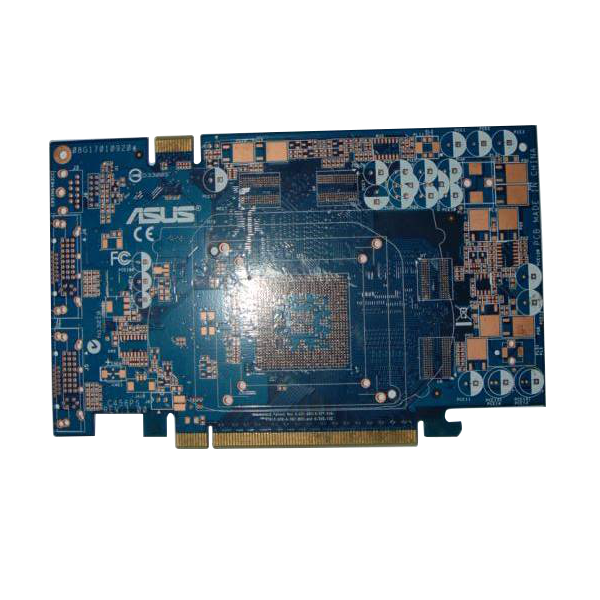
Multilayer PCBs are widely used across industries that demand reliability and performance.
High-quality multilayer PCBs must comply with international standards such as IPC and ISO certifications. Electrical testing, impedance control, and thermal stress testing are essential to ensure long-term reliability.
Akeson specializes in high-performance multilayer PCB manufacturing, offering customized solutions for complex electronic applications.
Multilayer PCBs typically range from 4 to over 40 layers, depending on application requirements.
While the initial cost is higher, multilayer PCBs often reduce overall system cost by saving space and improving performance.
Common materials include FR4, high-Tg laminates, and specialized high-frequency substrates.
If you are looking for reliable, high-performance multilayer PCB solutions tailored to your project, partner with Akeson today — contact us to discuss your requirements and get expert support.