
Akeson® is China manufacturer & supplier who mainly produces rogers4350 PCB High Quality High Frequency PCB Circuit Board with many years of experience.
Akeson® is a professional China rogers4350 PCB High Quality High Frequency PCB Circuit Board manufacturer and supplier
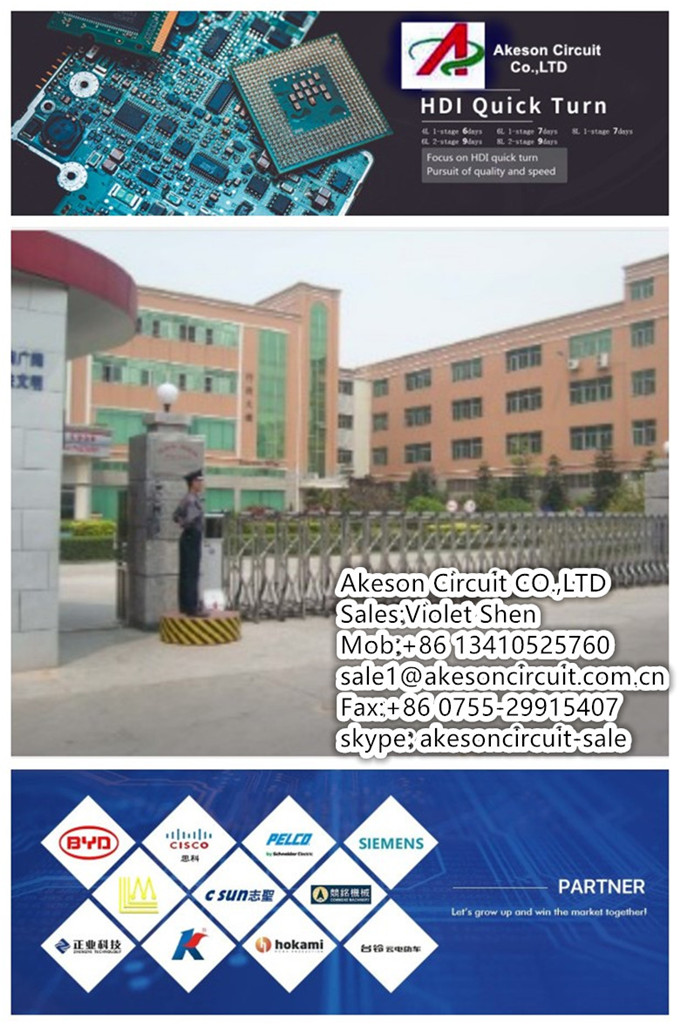
if have Gerber file or enquire. please email is violet(at)akesoncircuit(dot)com(dot) cn
Deliverables
1/Quotes in 24 hours or less
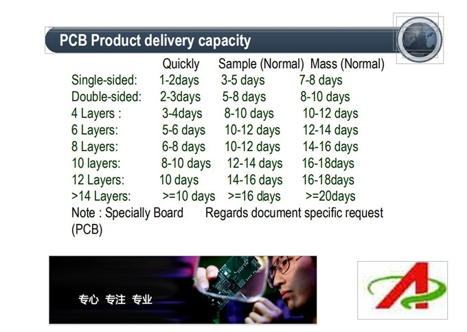
2/Standard production leadtime of 20 working days (4 weeks)
3/Prototype leadtime of 5 to 10 working days (1-2 weeks)
4/Stack-ups and impedance simulation in 36 hours
5/Initial response to technical questions or quality concerns in 36 hours
6/DFM and EQ's prior to PO placement upon request
Akeson® Quality system
1/Akeson has mature and stringent Q
2/100% AOI, 100% ET, 100% FQC + FQA
3/SPC and Cpk programs
4/Lean Manufacturing and 6S programs
5/Advanced inspection and lab equipment
6/Standard QA report with every shipment
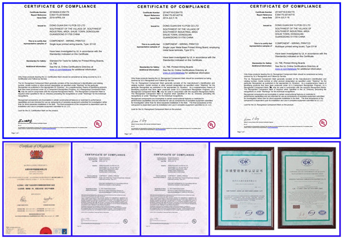
7/RoHS and REACH Compliance
8/Conflict Minerals Compliance
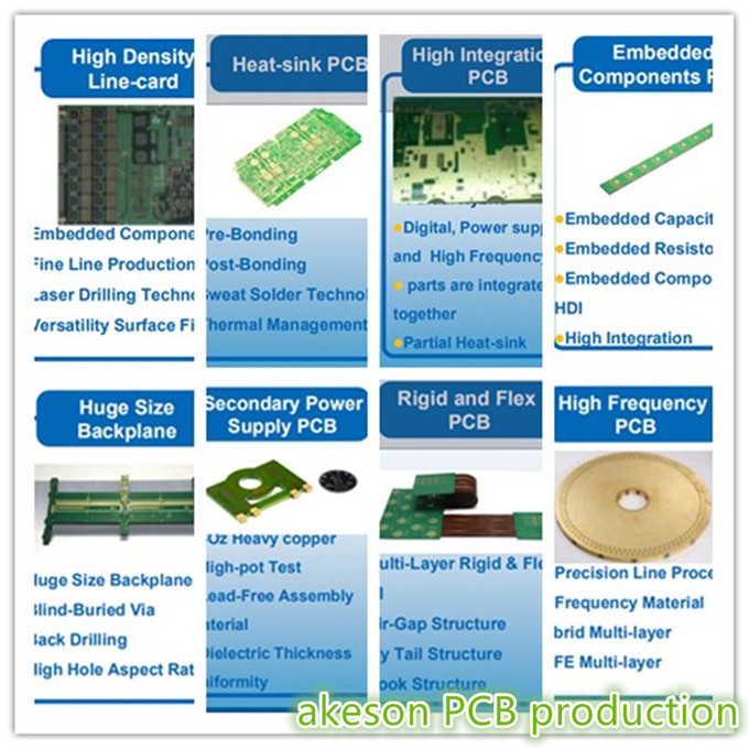
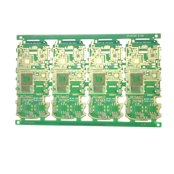
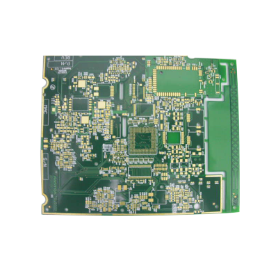
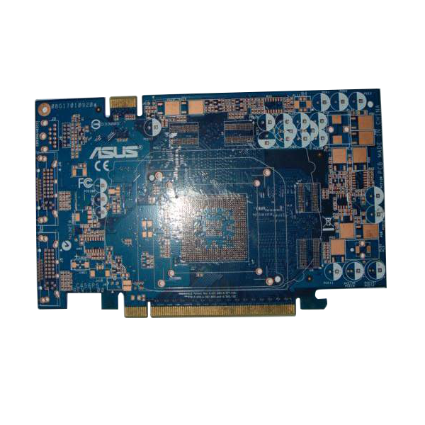
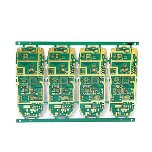
Products infomation
8 layer,
Material:FR4(Tg180) material,
PCB thickness:1.60mm thick,
Final copper:1 OZ finished copper on all layers,
Surface:ENIG surface finish,
Ttchnology:with hard gold finger at edge-board,
Solder mask:green solder mask,
with impedance control
6.0/7.0mil min w/s(line width/spacing),
min drill bit:0.20mm,
min BGA pad size:0.33mm
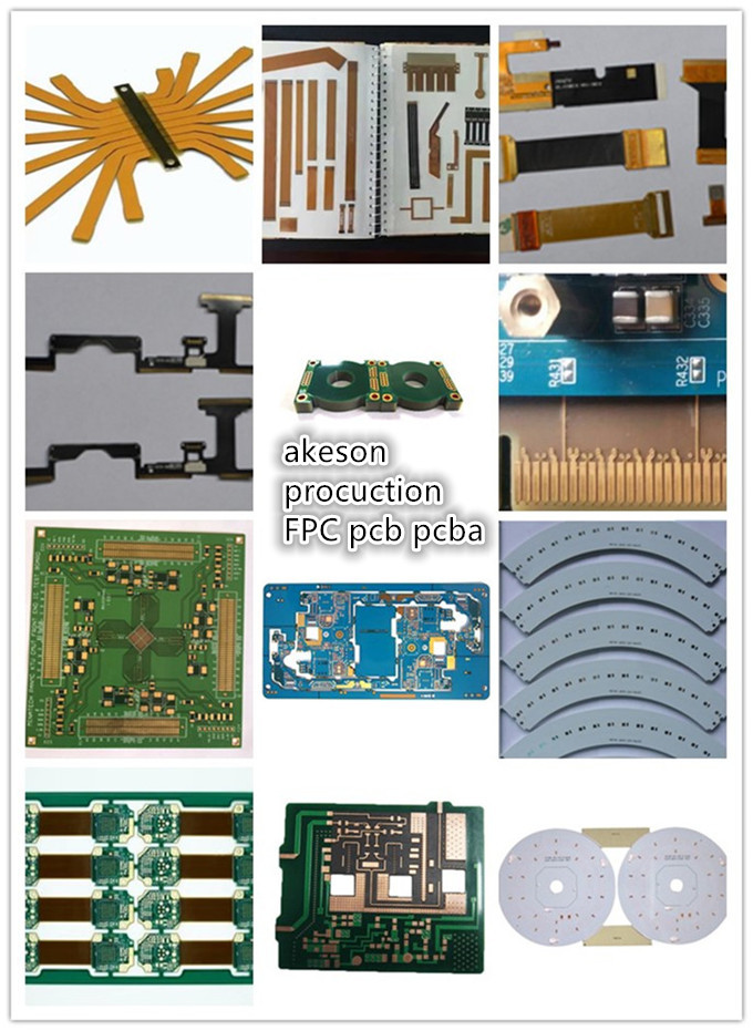
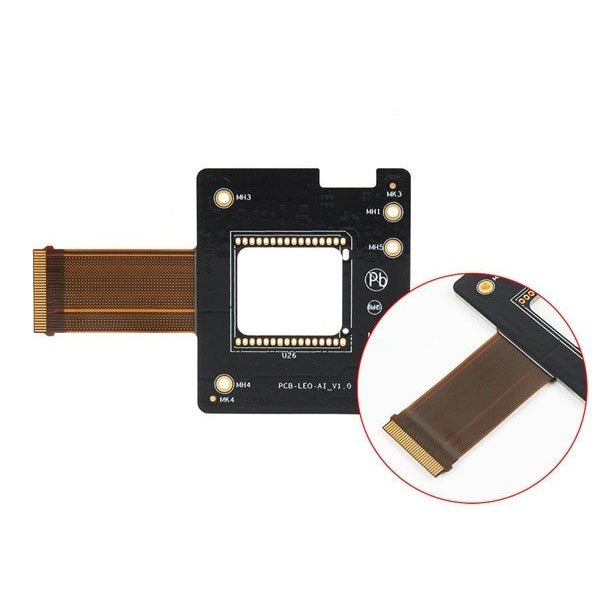
Double Side Flexible PCB PCB material we can use:
FR1, FR2, HB, CEM1, CEM3, FR4, High TG/CTI FR4, Halogen Free, Rogers, Aluminium based, Lead-free compatible, Hi Frequency
PCB Requested information for PCB assembly:
1. Gerber files of the bare PCB board
2. BOM (Bill of material) for assembly
3. Testing Guide & Test Fixtures if necessary
4. Schematic if necessary
5.Paypal available
If you can provide the Gerber file or sent a sample to us, our work will be easyer and can deliver to you within 10 days.
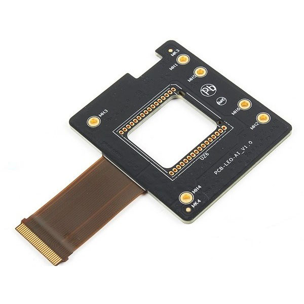
We can provide Akeson® FPC Board(1-8layer and rigid-flex:6layer max)
|
Technical Specification
|
|||
|
Materials
|
Polyimide/Polyester
|
Remark&Test Method
|
|
|
Number of Layer
|
FPCB 1-8/Rigid-flex:1-6
|
|
|
|
Min.Trace
Width/Space |
Single Side
|
0.050mm(2mil)
|
|
|
Double Side
|
0.050mm(2mil)
|
|
|
|
Min.Hole
Diameter |
Drilling(P.T.H.)
|
φ0.15mm
|
|
|
Punching
|
φ0.50mm
|
||
|
Dimension
Tolerance |
Conductor Width
|
20%
|
W≤0.5mm
|
|
Hole Diameter(H)
|
0.05mm
|
H≤1.5mm
|
|
|
Accumulated
Pitch |
0.05mm
|
P≤25mm
|
|
|
Outline Dimension
|
±0.1mm
|
L≤50mm
|
|
|
Conductors And
Outline |
±0.07mm
|
C≤5.0mm
|
|
|
Surface Treatment On Terminal
And Land Area |
Au(0.03-1.5um)
|
|
|
|
Ni(1-6um)
|
|||
|
Sn(7-20um)
|
|||
|
Peeling Strength(180° Direction)
|
1.0kg f/cm
|
IPC-TM-650 2,4,9
|
|
|
Solder Heat Resistance
|
260/10 secs
|
|
|