With years of experience in production Akeson® Multilayer pcb Tin-plated communication PCB 4L use Teflons pcb, Akeson can supply a wide range of Multilayer pcb Tin-plated communication PCB 4L use Teflons pcb.
Akeson® High quality Multilayer pcb Tin-plated communication PCB 4L use Teflons pcb can meet many applications, if you need, please get our online timely service about Multilayer pcb Tin-plated communication PCB 4L use Teflons pcb from China.
mulitlayer pcb Tin-plated communication PCB 4L use Teflon pcb Multilayer pcb Tin-plated communication PCB 4L use Teflons pcb
We maintain high standards of excellence, strive for 100% customer's satisfaction and response within 24 hours
Send us: PCB/Gerber files, PCB requirements, BOM list, assembly or soldering technical requirements
PCB Bare Board:
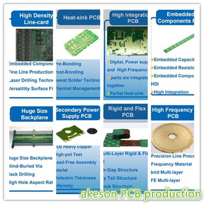
Multi-layer,FR4,Metal,Creamic,Rogers,FPC,HDI board.
HASL,Immersion Gold/silver/Au,OSP, etc.
PCB Assembly:
9 Testing Procedures,100% Functional Tested.
BGA with X-Ray and Lead Free Assembly.
Components Sourcing:
15 Years Purchasing Experience.
Multi-channel Component Supply.
Finished products assembly:
Functional test/Programing.
Conformal Coating. Burning test.
Gift Box Packing. Storege Service.
Our advantages:
1, Online 360° Panoramic View Factory.
2, National High-tech Enterprise.
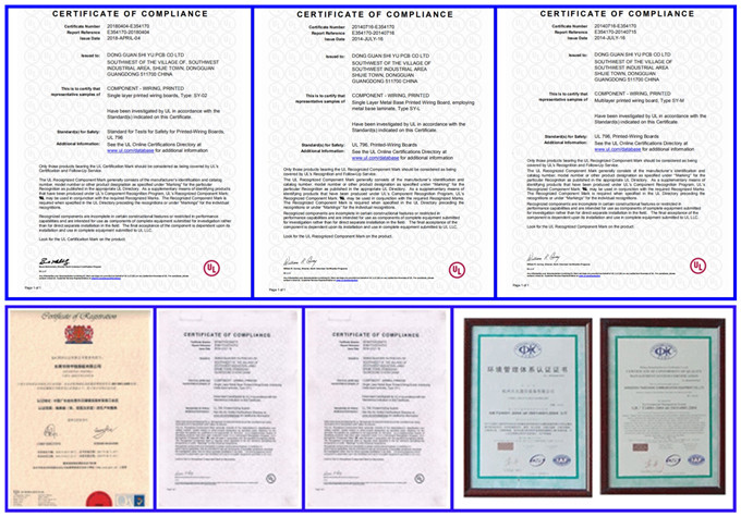
3, ISO9001, ISO13485, IATF16949 Certification.
4, Customade ERP To Control The Process.
5, No MOQ, Flexible Service.
Contact us to get quotation.
if have Gerber file or enquire. please email is violet(at)akesoncircuit(dot)com(dot) cn
Deliverables
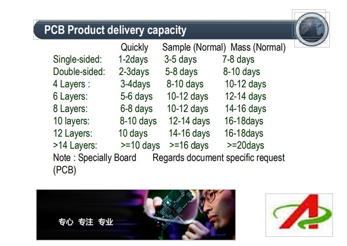
1/Quotes in 24 hours or less
2/Standard production leadtime of 20 working days (4 weeks)
3/Prototype leadtime of 5 to 10 working days (1-2 weeks)
4/Stack-ups and impedance simulation in 36 hours
5/Initial response to technical questions or quality concerns in 36 hours
6/DFM and EQ's prior to PO placement upon request
Quality system
1/Akeson has mature and stringent Q
2/100% AOI, 100% ET, 100% FQC + FQA
3/SPC and Cpk programs
4/Lean Manufacturing and 6S programs
5/Advanced inspection and lab equipment
6/Standard QA report with every shipment
7/RoHS and REACH Compliance
8/Conflict Minerals Compliance
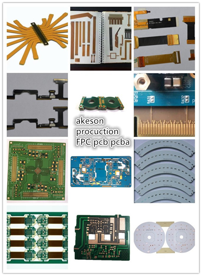
Flexible PCB(FPC)
1. Layer: 1-8 layer
2. Max panel size: 1000mm*500mm
3. Min Board thickness: Single sided: 0.06mm, Double sided: 0.10mm, Three sided: 0.20, Four sided: 0.26mm, Five sided: 0.32mm, six sided: 0.06mm
4. Min line width/space: 3mil/3mil
5. Min hole size: 0.15mm
6. Surface finishing: Chemical Gold, Immersion Gold, OSP, Immersion AG
7. Material: Copper thickness: 1/4oz, 1/2oz, 1oz, 1.5oz, 2oz PI thickness: 1/2mil
8. Assembly: SMT
Provided FPC, flexible PCB OEM/ODM, PCB fabrication, PCB assembly, PCB test, component parts purchase^^
PCB material we can use:
FR1, FR2, HB, CEM1, CEM3, FR4, High TG/CTI FR4, Halogen Free, Rogers, Aluminium based, Lead-free compatible, Hi Frequency
PCB Requested information for PCB assembly:
1. Gerber files of the bare PCB board
2. BOM (Bill of material) for assembly
3. Testing Guide & Test Fixtures if necessary
4. Schematic if necessary
5.Paypal available
If you can provide the Gerber file or sent a sample to us, our work will be easyer and can deliver to you within 10 days.
FPCA/PCBA production:
We can provide all type of PCBa/FPCA production"
1) Dynamic flexing requirements
2) Reduce space
3)Light weight
4) Provide uniform electrical characterisitics for high speed circuitry
5) Flexing for easier installation
6) Good insulation
|
Number of Layer |
|
1~8(Rigid-Flex & Multilayers FPC) |
|
|
Min. Track Width/Spacing |
Single Sided |
0.030 mm / 0.040 mm |
|
|
Double Sided |
0.030 mm / 0.050 mm |
|
|
|
Min. Hole Diameter |
Drilling P.T.H. |
0.2 mm |
|
|
Punching |
1.0 mm |
|
|
|
Dimension Tolerances |
Conductor Width (W) |
0.020 mm |
W0.5mm |
|
Hole Diameter (H) |
0.05 mm (withP.T.H.0.1mm) |
H1.5mm |
|
|
Accumulated Pitch (P) |
0.015 mm |
P25mm |
|
|
Outline Dimension (L) |
0.05 mm |
L50 mm |
|
|
Conductors and Outline (C) |
0.15 mm (Special 0.07mm) |
C5.0 mm |
|
|
Conductors and Coverlay |
0.3~0.5 mm |
|
|
|
Surface Treatment on Terminals and land Areas |
Soft or Hard Ni/Au Sn/Pb (2~60μm) Primary FluxCarbon Printed (4~10μm Silver Gel printed |
|
|
|
Insulation Resistance |
1000MW |
IPC-TM-650 2.6.3.2 at Ambient |
|
|
Dielectric Strength |
5KV |
IPC-TM-650 2.5.6.1 |
|
|
Surface Resistance (W) |
5x012 |
IPC-TM-650 2.5.17 |
|
|
Volume Resistivity (W-cm) |
1x015 |
IPC-TM-650 2.5.17 |
|
|
Dielectric Constant (1 MHz) |
4.0 |
IPC-TM-650 2.5.5.3 |
|
|
Dissipation Factor (1 MHz) |
0.04 |
IPC-TM-650 2.5.5.3 |
|
|
Peeling Strength (180 irection) |
1.2kgf/cm |
IPC-TM-650 2.4.9 |
|
|
Solder Heat Resistance |
260 .C/10secs |
|
|
|
Flammability |
94 V-0 |
UL94 |
|
|
Water Absorption |
2.9% |
ASTM D570% |
|
