HDI PCB (High Density Interconnect Printed Circuit Board) technology has become a cornerstone of modern electronic design. As electronic devices become smaller, faster, and more powerful, traditional PCBs often struggle to meet the demands of compact layouts and high-speed performance. HDI PCBs solve this challenge through microvias, fine traces, and advanced layer stacking.
In this comprehensive guide, we explore what HDI PCBs are, how they work, their advantages, manufacturing processes, applications, and why they are crucial for next-generation electronics. This article also highlights how manufacturers such as Akeson help deliver reliable HDI PCB solutions for industries ranging from consumer electronics to medical devices.

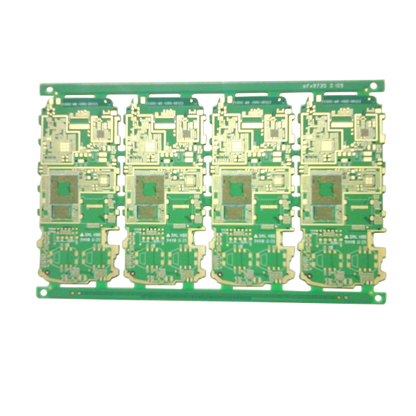
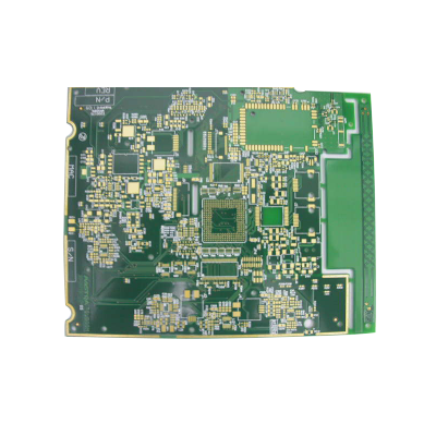
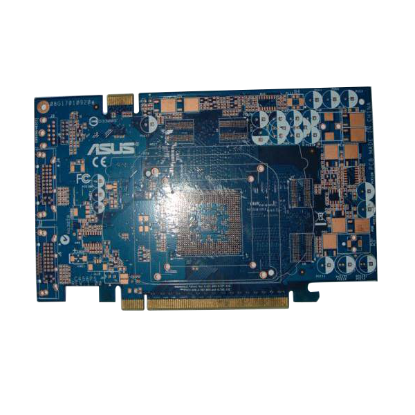
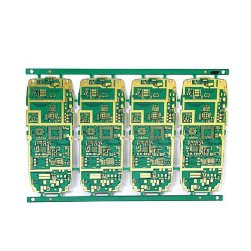
HDI PCB stands for High Density Interconnect Printed Circuit Board. It is a type of circuit board that features higher wiring density per unit area compared to conventional PCBs. HDI boards achieve this through advanced technologies such as microvias, blind vias, buried vias, and fine trace routing.
The goal of HDI PCB design is to allow more components to fit within a smaller area while maintaining excellent electrical performance. This makes HDI PCBs ideal for compact electronic products such as smartphones, tablets, wearable devices, and advanced computing equipment.
If you want to explore a professional HDI PCB solution, you can learn more about HDI PCB technology and services offered by leading manufacturers.
Compared with standard multilayer PCBs, HDI boards use advanced laser drilling and sequential lamination processes, enabling extremely small vias and high-density routing.
Modern electronic devices demand greater functionality within increasingly smaller spaces. Traditional PCB designs often struggle to support the high component density and signal speed required by modern electronics.
HDI PCB technology solves this challenge by enabling:
Without HDI PCBs, many of today’s advanced devices such as high-performance smartphones, AI processors, and medical equipment would be significantly larger and less efficient.
HDI PCBs incorporate several advanced design and manufacturing features that distinguish them from traditional circuit boards.
| Feature | Description |
|---|---|
| Microvias | Laser-drilled vias smaller than 150 microns used to connect layers |
| Fine Line Routing | Narrow copper traces allowing more circuits within limited space |
| Sequential Lamination | Layer-by-layer lamination enabling complex multilayer structures |
| High Layer Count | Supports advanced electronic designs with multiple layers |
| Improved Signal Integrity | Shorter signal paths reduce interference and improve performance |
Manufacturers like Akeson focus on precision fabrication technologies to ensure HDI PCBs meet strict quality and performance standards.
HDI PCBs typically consist of several types of vias and layer configurations.
These via structures allow engineers to optimize signal routing while maintaining a compact board size.
Producing HDI PCBs requires advanced equipment and highly controlled manufacturing processes.
High-end facilities such as those operated by Akeson ensure HDI PCB boards meet stringent performance requirements for modern electronics.
HDI PCBs provide several critical advantages compared with conventional PCBs.
These benefits make HDI PCBs ideal for high-performance applications requiring both compact design and reliability.
| Aspect | HDI PCB | Traditional PCB |
|---|---|---|
| Via Size | Microvias | Standard drilled vias |
| Routing Density | Very High | Moderate |
| Signal Performance | High-speed capable | Limited high-speed capability |
| Board Size | Compact | Larger |
| Manufacturing Complexity | Advanced | Standard |
While HDI boards require more advanced fabrication techniques, their performance advantages make them essential for modern electronics.
HDI PCBs are widely used across many industries where compact design and high-speed performance are essential.
As electronic systems become more integrated and powerful, the demand for HDI PCBs continues to increase globally.
Selecting the right manufacturer is crucial for ensuring quality and reliability in HDI PCB production.
Companies like Akeson specialize in high-quality HDI PCB manufacturing and provide comprehensive technical support for complex electronic projects.
The HDI PCB industry continues to evolve as electronic devices demand greater performance and miniaturization.
These innovations will further expand the role of HDI PCBs in next-generation electronics and communication systems.
HDI stands for High Density Interconnect. It refers to circuit boards that use microvias and fine traces to achieve higher wiring density compared with traditional PCBs.
Smartphones require compact circuit boards capable of supporting powerful processors and high-speed communication modules. HDI PCBs allow more components to fit into a smaller space while maintaining reliable performance.
HDI PCBs generally cost more than traditional PCBs due to advanced manufacturing processes such as laser drilling and sequential lamination. However, their performance and space-saving advantages often justify the investment.
Common materials include FR-4, high-speed laminates, polyimide, and advanced dielectric materials designed to support high-frequency signals.
When properly manufactured, microvias are highly reliable and widely used in high-performance electronic devices worldwide.
HDI PCB technology has revolutionized modern electronics by enabling smaller, faster, and more powerful devices. Through advanced manufacturing processes such as microvia drilling and sequential lamination, HDI PCBs provide superior routing density and signal integrity compared with traditional boards.
As industries continue to push the limits of electronic performance and miniaturization, HDI PCBs will remain a fundamental component of innovation.
If you are looking for professional HDI PCB solutions, the experienced engineering team at Akeson can provide reliable manufacturing, customized design support, and high-quality production to meet the needs of modern electronic applications.
Looking for high-performance HDI PCB manufacturing services? Contact us today to discuss your project and discover how our advanced PCB solutions can support your next innovation.