Article Summary: High Density Interconnect (HDI) board electronic prototyping boards are transforming how engineers design, test, and launch advanced electronic products. With the growing demand for compact devices, faster signal transmission, and complex multilayer circuit designs, HDI technology has become a critical solution in modern electronics manufacturing. This comprehensive guide explores the advantages, structure, applications, design considerations, and prototyping processes of HDI boards. It also explains how companies like Akeson support engineers with reliable HDI prototyping services that accelerate innovation and reduce development risks.

HDI board electronic prototyping boards refer to high-density interconnect printed circuit boards used for prototype development. These boards incorporate advanced PCB manufacturing techniques such as microvias, blind vias, buried vias, and ultra-fine trace routing to achieve higher component density.
Unlike traditional PCBs, HDI boards are designed to support compact electronic systems where space efficiency and signal integrity are critical. They allow engineers to prototype complex devices before full-scale production.
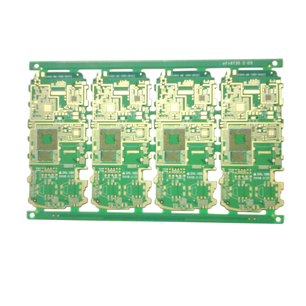
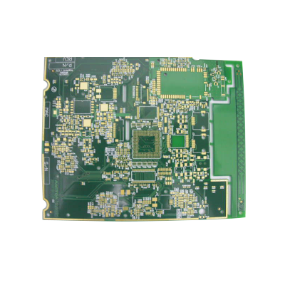
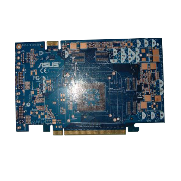
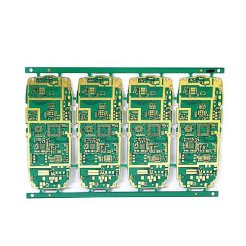
Typical HDI prototyping boards include:
For engineers developing next-generation electronics, HDI prototypes serve as the testing platform that validates circuit functionality and performance before mass manufacturing.
Modern electronics continue to shrink in size while increasing in functionality. Smartphones, wearable devices, medical instruments, and IoT systems all require compact yet powerful circuit architectures.
HDI technology enables these innovations by allowing more circuits to fit into smaller spaces.
When developing prototypes, using HDI boards ensures that the final product design meets modern engineering standards.
The unique performance of HDI boards comes from their structural design and manufacturing processes.
| Feature | Description | Benefit |
|---|---|---|
| Microvias | Laser-drilled vias smaller than 150μm | Higher routing density |
| Blind Vias | Connect outer layers to inner layers | Improved board space usage |
| Buried Vias | Internal layer connections | Reduced signal interference |
| Sequential Lamination | Layer-by-layer lamination process | Supports complex multilayer structures |
| Fine Trace Routing | Extremely narrow copper traces | Allows dense component layouts |
These advanced structures allow HDI boards to handle complex electronic systems that traditional PCBs cannot support efficiently.
Understanding the difference between HDI boards and standard PCBs helps designers choose the right solution for their prototypes.
| Characteristic | HDI PCB | Traditional PCB |
|---|---|---|
| Trace Width | Ultra-fine traces | Standard trace widths |
| Via Technology | Microvias, blind, buried | Through-hole vias |
| Component Density | Very high | Moderate |
| Board Size | Compact | Larger footprint |
| Signal Performance | High-speed capable | Limited for high-speed signals |
For complex electronics such as smartphones or advanced computing systems, HDI boards are the preferred choice.
HDI board electronic prototyping offers several advantages for engineers and product developers.
These advantages make HDI boards a preferred option for prototype development in cutting-edge industries.
HDI boards are widely used across many industries where electronic devices require high performance and compact structures.
Each of these applications requires circuit boards capable of handling high-speed data transmission and dense component layouts.
Producing HDI prototyping boards involves advanced manufacturing techniques.
Manufacturers like Akeson specialize in advanced HDI board fabrication to ensure consistent prototype quality and reliable electrical performance.
Designing HDI boards requires careful planning and engineering expertise.
Following proper design guidelines helps ensure that the prototype performs reliably during testing and evaluation.
Selecting the right supplier plays a critical role in the success of electronic prototyping projects.
Companies such as Akeson provide professional HDI board prototyping solutions designed to meet the demanding requirements of modern electronics development.
The future of HDI PCB technology will continue evolving alongside emerging electronics innovations.
As electronic devices become smarter and smaller, HDI boards will remain essential for supporting complex circuit architectures.
HDI stands for High Density Interconnect, a PCB design approach that uses microvias and fine traces to achieve higher circuit density.
HDI boards allow engineers to test compact and complex circuit designs before entering mass production.
HDI boards typically cost more than traditional PCBs due to advanced manufacturing processes, but they provide superior performance and space efficiency.
Industries including telecommunications, automotive electronics, medical devices, and consumer electronics widely use HDI boards.
HDI boards can range from 4 layers to more than 20 layers depending on the complexity of the electronic design.
HDI board electronic prototyping boards play a critical role in modern electronics development. Their ability to support high-density circuits, compact device designs, and high-speed signal performance makes them essential for next-generation technology.
From smartphones and medical devices to advanced communication systems, HDI boards enable engineers to transform complex ideas into functional prototypes quickly and efficiently.
If you are looking for professional HDI board manufacturing and prototyping solutions, Akeson offers reliable production capabilities, engineering expertise, and high-quality PCB solutions tailored to modern electronics innovation.
Interested in high-quality HDI board electronic prototyping boards for your next project? Contact us today to explore customized PCB solutions and accelerate your product development.