Article Summary: HDI PCB (High Density Interconnect Printed Circuit Board) has become a cornerstone technology in modern electronics, enabling smaller, lighter, and more powerful devices. This in-depth guide explains what HDI PCB is, how it works, its structure types, manufacturing process, advantages over traditional PCBs, and why industries such as consumer electronics, automotive, medical, and industrial automation increasingly rely on it. The article also explores design considerations, cost factors, and how to choose a reliable HDI PCB manufacturer like Akeson.
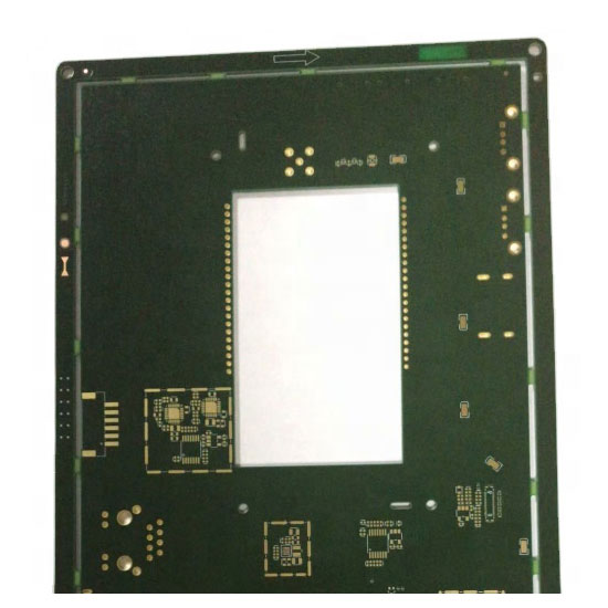
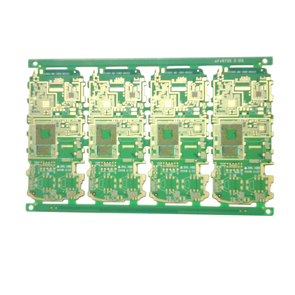
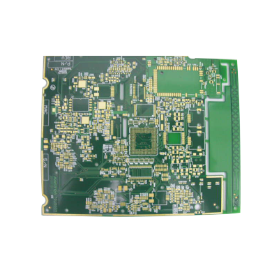
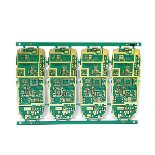
An HDI PCB (High Density Interconnect Printed Circuit Board) is a type of advanced circuit board characterized by higher wiring density per unit area compared to conventional PCBs. HDI PCBs use technologies such as microvias, blind vias, buried vias, laser drilling, fine lines, and thin materials to achieve superior electrical performance and miniaturization.
Unlike traditional PCBs that rely on mechanically drilled through-holes, HDI PCBs employ laser-drilled microvias, typically with diameters smaller than 150 microns. This allows components to be placed closer together, reducing board size while increasing functionality.
Modern electronic devices demand:
HDI PCB technology directly addresses these demands. Without HDI PCBs, products such as smartphones, wearables, high-performance medical devices, and advanced automotive electronics would not be feasible.
As semiconductor packaging continues to evolve (BGA, CSP, flip-chip), HDI PCBs provide the necessary interconnection density to support these components efficiently.
| Feature | HDI PCB | Traditional PCB |
|---|---|---|
| Via Type | Microvias, blind & buried vias | Through-hole vias |
| Line Width/Spacing | ≤ 3/3 mil or finer | Typically ≥ 6/6 mil |
| Board Size | Highly compact | Larger footprint |
| Signal Integrity | Excellent for high-speed signals | Limited at high frequencies |
| Manufacturing Complexity | High | Moderate |
HDI PCBs are commonly classified based on the number of buildup layers:
Any Layer HDI represents the most advanced structure, offering maximum routing flexibility and density.
The manufacturing of HDI PCBs involves multiple precision-controlled steps:
Due to the complexity, HDI PCB manufacturing requires advanced equipment, strict process control, and experienced engineering teams—capabilities that professional suppliers like Akeson continuously invest in.
HDI PCBs are widely used across industries:
Successful HDI PCB design requires careful planning:
Early collaboration with your PCB manufacturer can significantly reduce cost and lead time.
While HDI PCBs offer exceptional performance, they come at a higher cost due to:
However, the overall system cost is often reduced thanks to smaller board sizes, fewer layers, and improved reliability.
When selecting an HDI PCB supplier, consider the following:
Akeson provides end-to-end HDI PCB solutions, from design support to volume manufacturing, ensuring consistent quality and reliable delivery.
All HDI PCBs are multilayer PCBs, but not all multilayer PCBs are HDI. HDI focuses on higher density using microvias and fine lines.
Yes. HDI PCBs offer excellent signal integrity, making them ideal for high-speed and high-frequency applications.
Common finishes include ENIG, ENEPIG, OSP, immersion silver, and immersion tin.
With mature processes and automation, HDI PCBs are widely used in high-volume consumer electronics manufacturing.
Conclusion:
HDI PCB technology has become indispensable in modern electronics, enabling innovation, miniaturization, and high performance across industries. Choosing the right HDI PCB partner ensures product reliability, cost efficiency, and long-term success.
If you are looking for a trusted HDI PCB solution provider with strong engineering capabilities and manufacturing expertise, Akeson is ready to support your project — contact us today to discuss your requirements.