Mobile Phone PCB Circuit Boards PCB
  • Mobile Phone PCB Circuit Boards PCBMobile Phone PCB Circuit Boards PCB

Mobile Phone PCB Circuit Boards PCB

Akeson® is Mobile Phone PCB Circuit Boards PCB Layout 6Layer Multilayer PCB and PCBA manufacturers and suppliers in China who can wholesale Mobile Phone PCB Circuit Boards PCB Layout 6Layer Multilayer PCB and PCBA.

Send Inquiry

Product Description

Akeson® Mobile Phone PCB Circuit Boards PCB Layout 6Layer Multilayer PCB and PCBA Manufacturer 


if have Gerber file or enquire. please email is violet(at)akesoncircuit(dot)com(dot) cn

Deliverables
1/Quotes in 24 hours or less 
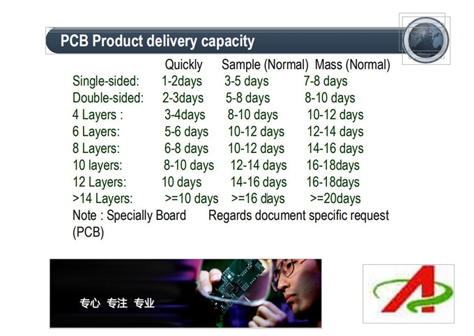
2/Standard production leadtime of 20 working days (4 weeks)
3/Prototype leadtime of 5 to 10 working days (1-2 weeks)
4/Stack-ups and impedance simulation in 36 hours
5/Initial response to technical questions or quality concerns in 36 hours
6/DFM and EQ's prior to PO placement upon request
Quality system
1/Akeson has mature and stringent Q
2/100% AOI, 100% ET, 100% FQC + FQA
3/SPC and Cpk programs
4/Lean Manufacturing and 6S programs
5/Advanced inspection and lab equipment
6/Standard QA report with every shipment
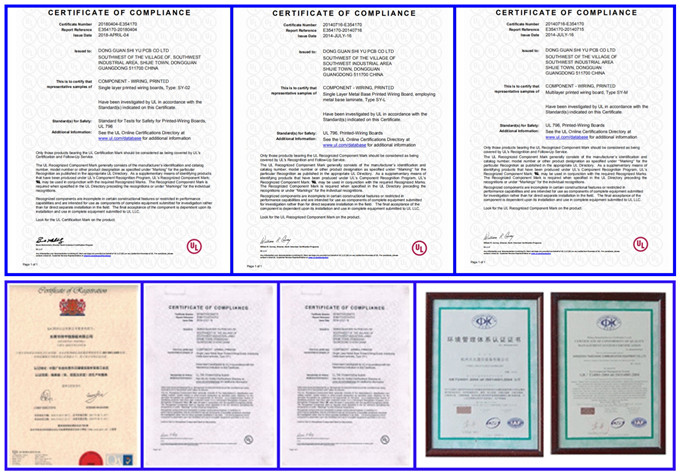
7/RoHS and REACH Compliance
8/Conflict Minerals Compliance
 
Akeson® pcb assembly
 
1) Layer: 6 layer pcb assembly
2) Board finished thickness: 1.6mm
3) Material: FR-4
4) Min. drilled hole size: 0.4mm
5) Min. Line width: 4mil (0.1mm)
6) Min.Line spacing: 4mil (0.1mm)
7) Surface finish/treatment: immersion gold
8) Copper thickness: 1 OZ
10) Solder mask color: green
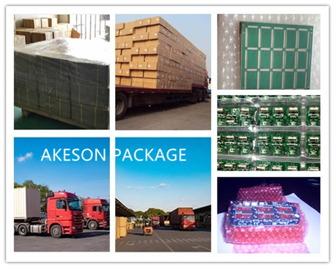
11)Inner packing: Vacuum packing / Plastic bag
Outer packing: Standard carton packing
12) Sample or mass produce, 4 days lead time
13) OEM/ODM is acceptable
 
 
Reference - Our Production Capability for Multilayer PCB/Rigid borad
 
Item
 
M-
Layer count
1-30 layers
Material
FR4(High TG, Halogen Free, high frequency), CEM1, CEM3,BT,Al base mateiral,and so on.
Supplier: SY,KB,ITEQ,Isola,Nelco,Rogers,Grance,Mitsui
Maxpanel size
32±20(800mm±508mm)
Min width/space(min)
4mil/4mil
Max copper weight
140um(4oz) for inner layer
175um(5oz) for outer layer
Min machine drill size
0.2mm(8mil)
Via hole tpye
Blind/Burried/plugged
Thickness of finished board
0.20-6.0mm
Tolerance
Registration of innerlayer to of innerlayer:±3mil
Accuracy of hole position:±2mil
Tolerance of dilled slot:±3mil
Tolerance of PTH diameter:±3mil
Tolerance of NPTH diameter:±2mil
PTH hole copper thichness: 0.4-2mil
Image to image tolerance:±3mil
Tolerance of etching:±1mil
Solder mask registration tolerance: ±2mil
Finished board : Thickness<=1.0mm: +/-0.1mm
Thickness>0.1mm:+/-10%
Outline router: +/-0.1mm
Outline Score: +/-0.2mm
Color of solder mask
Green, Black, Blue,Red, White and so on
Surface freatment
HASL,HASL Lead Free,OSP ,Immersion Gold, Immersion Ti, Immersion Sliver, Flash gold, Selective Gold plating(gold thicness up to 120u),Gold figers ,Carbon print, Peelabe Mask
Hardness of solder solder
>=6H
Outline finished
CNC, V-CUT, Punching
Peel strength of line
≥61B/in
Warp and twist
≤0.7%


Hot Tags: Mobile Phone PCB Circuit Boards PCB, China, Manufacturers, Suppliers, Factory, Customized

Product Tag

Related Category

Send Inquiry

Please Feel free to give your inquiry in the form below. We will reply you in 24 hours.