PCBA Design is the foundation of modern electronic product development. From schematic capture and PCB layout to DFM optimization and assembly validation, a professional PCBA design process directly impacts performance, reliability, cost, and speed to market. In this comprehensive guide, we explore how advanced PCBA design services enhance manufacturing efficiency, reduce risks, and accelerate innovation. Whether you are developing IoT devices, industrial controllers, or consumer electronics, understanding the full PCBA workflow is critical for long-term product success.

PCBA Design refers to the complete engineering process of designing a Printed Circuit Board Assembly (PCBA), which includes schematic development, PCB layout, component selection, signal routing, thermal analysis, power management, and preparation for manufacturing and assembly.
Unlike simple PCB layout, PCBA design considers the entire lifecycle of the electronic product:
A professional PCBA design service, such as those offered by Akeson PCBA Design Services, integrates engineering, procurement, and manufacturing expertise into a unified development solution.
Poor PCBA design can result in signal interference, overheating, production delays, component mismatch, and costly redesigns. On the other hand, optimized PCBA engineering significantly improves:
| Design Factor | Impact on Final Product |
|---|---|
| Signal Integrity | Ensures stable data transmission and reduced EMI |
| Thermal Management | Prevents overheating and extends product lifespan |
| Component Placement | Improves assembly efficiency and reduces defects |
| Power Distribution | Enhances performance stability |
| DFM Optimization | Lowers manufacturing cost and increases yield rate |
By working with experienced engineering teams like Akeson, companies can minimize development risks and accelerate commercialization.
Understanding product specifications, voltage levels, communication protocols, mechanical constraints, and regulatory requirements.
Engineers create detailed circuit diagrams, defining component connections and functionality.
This stage includes:
Signal integrity analysis, power integrity analysis, and thermal simulations reduce prototype iterations.
Ensuring the design is ready for SMT assembly and mass production.
Functional testing, debugging, and validation before full-scale production.
Design for Manufacturing (DFM) ensures that the PCBA can be produced efficiently with minimal defects. Key DFM considerations include:
DFM integration reduces:
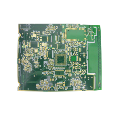
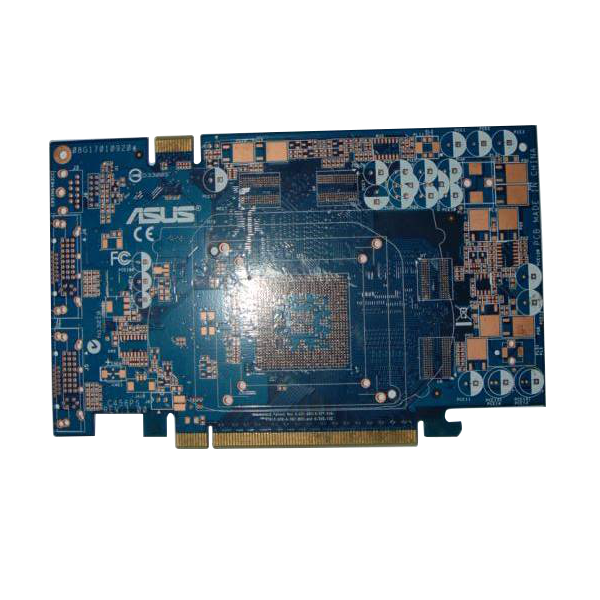
Advanced PCBA development leverages cutting-edge tools and technologies:
| Technology | Application |
|---|---|
| High-Speed PCB Design | 5G, IoT, and communication devices |
| HDI PCB Layout | Compact consumer electronics |
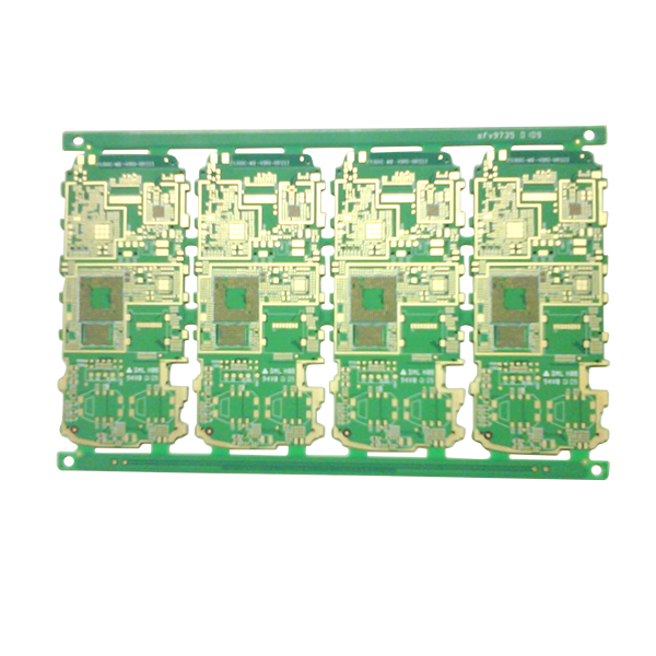
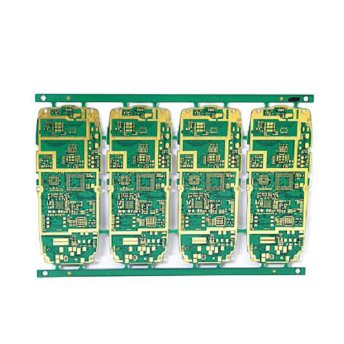
| Multilayer PCB (4–12 layers) | Industrial control systems |
| SMT Optimization | Automated assembly lines |
| Thermal Simulation | Power electronics and LED drivers |
Turnkey PCBA services integrate:
Benefits include:
Akeson provides integrated PCBA design and manufacturing services that help startups and enterprises bring products to market efficiently and reliably.
Consider the following criteria:
A professional partner like Akeson ensures technical excellence, manufacturing compatibility, and global delivery support.
PCB design focuses on board layout, while PCBA design includes component selection, assembly planning, and manufacturing readiness.
Depending on complexity, it typically ranges from 2–8 weeks including prototyping and testing.
Gerber files, BOM (Bill of Materials), Pick-and-Place files, assembly drawings, and test requirements.
DFM ensures the design can be manufactured efficiently with high yield and low defect rates.
Yes. Many turnkey providers support both prototype and mass production runs.
PCBA Design is more than circuit layout—it is the strategic engineering backbone of electronic product success. From schematic capture to mass production optimization, professional PCBA design services dramatically improve reliability, manufacturability, and market competitiveness.
If you are looking to develop innovative electronic products with higher performance and lower risk, Akeson provides comprehensive PCBA design and manufacturing solutions tailored to your needs.
Ready to accelerate your electronic product development? Contact us today to discuss your PCBA design project and discover how our engineering expertise can turn your concept into a market-ready solution.